


Since the introduction of monitoring adapters such as the WireView (Pro), the Ampinel or even NVIDIA’s PCAT, the same question keeps cropping up in forums and discussions: Do these devices cause a loss of performance in graphics cards because the built-in shunt resistors cause a minimal voltage drop? This concern persists, although no one has yet been able to provide valid proof of such an effect under controlled conditions. Urban legend or reality?

That’s why I set out to find out. In my lab today, I’m using four generations of AMD graphics cards and current NVIDIA graphics cards to test whether the additional measurement path actually has an impact on performance or whether it’s just a theoretical concern that doesn’t play a role in practice. The aim is to finally clarify the question of whether devices such as the older TG WireView or the new TG WireView Pro 2 as well as the Ampinel from Aqua Computer cost measurable performance, or whether the supposed disadvantage is simply a myth.
In order to properly understand the current problem, we first need to look at how the major GPU manufacturers have implemented their performance limitation and telemetry in the first place. Because only when it is clear where and how the respective card records its power consumption can it be understood whether an additional adapter with shunt resistors plays a role at all or not. Let’s take a look at exactly that now: How does NVIDIA really measure its board power, how did AMD solve this in older generations, and what has changed technically with RDNA 4? Only with this understanding can we assess whether the minimal voltage drop of an external measurement adapter could theoretically interfere with the power regulation, or whether this concern is simply unfounded.
Measurement and control concepts at AMD and NVIDIA – a comparison of old and new generations
The question of whether an external adapter with shunt resistors such as the WireView Pro or Ampinel measurably reduces GPU performance depends directly on how the respective graphics card measures and regulates its power consumption internally. AMD and NVIDIA differ here in terms of implementation, but both now rely on real current measurements via physical shunts directly on the board.
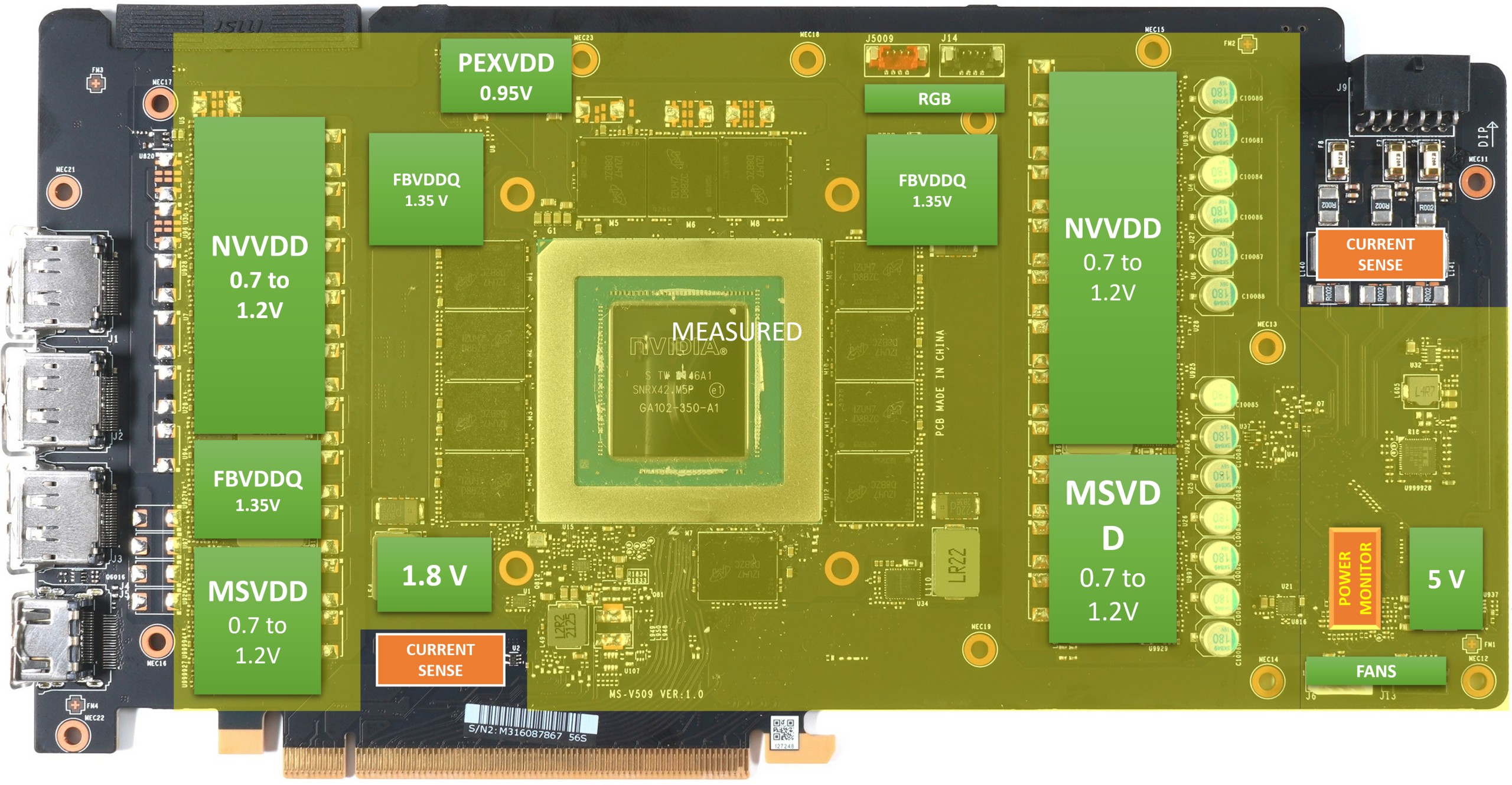
For years, NVIDIA has been measuring the board power via low-impedance shunt resistors integrated into the 12 V feeds (PCIe slot, 6/8-pin connector, or 12VHPWR/12V-2×6). Each shunt generates a minimum voltage drop proportional to the current (ΔV = I-R), which is recorded by the PMU via differential ADC inputs. These values are used to calculate the current, voltage and ultimately the total board power. The PMU uses this real measurement to regulate the GPU boost behavior: As soon as the sum of the shunt measurements reaches the specified limit (TGP/TBP), the board reduces the voltage or clock. This means that NVIDIA’s performance limitation is closely linked to physical values.
AMD older generations: Power estimation via VRM telemetry
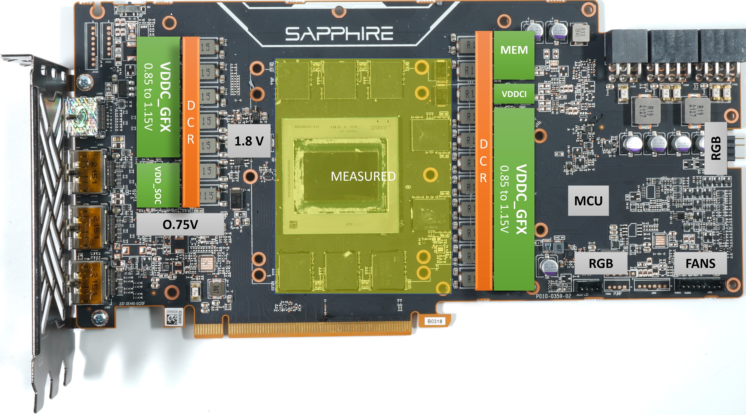
Earlier AMD generations, especially up to RDNA 3, primarily used estimation models (power estimation) based on the voltage and current values that the VR controllers of the GPU rails (VDDCR_GFX, VDD_SOC, VDD_MEM etc.) reported to the SMU via the SVI2/3 bus. As no shunts and monitoring chips are installed on the AMD cards, the firmware has to obtain the data differently. This is done using data that all graphics cards have. Instead, the values of the currents are simply used, which all relevant voltage converters supply anyway. This is done at the output of the phases, i.e. AFTER all the losses that occur. A special procedure is required to ensure the balance of the phases and to be able to control the individual control loops. The keyword is DCR (Direct Current Resistance). And now we also understand that this data, which is only collected locally, is incomplete because it does not even include the fans, let alone the other installed electronic consumers and PCB losses.

The current was measured after the voltage conversion (i.e. behind the VRMs). Losses in the VRMs or in the 12 V supply line were not taken into account in this telemetry. The method is precise for the chip power consumption, but only approximates the board power. AMD’s power limitation was therefore primarily based on model values, not real shunt measurements of the input current paths.
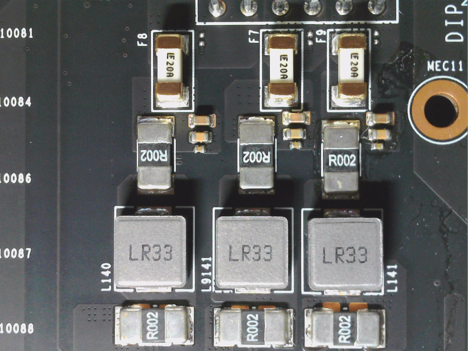
AMD newer generation (RDNA4) and Intel’s BMG: Shunts like NVIDIA
With RDNA 4, AMD uses real shunt resistors to measure the input currents on the board, similar to NVIDIA. Typically, these shunts are located in the 12 V feeds of the PCIe slot and on the external power connectors. The values are captured via precision ADC front-ends and consolidated in the SMU, providing the board with real board power capture. The boost logic incorporates both GPU rail power (SVI values) and board shunt power. AMD has thus closed the gap between “power estimation” and real physical power limitation. This means that RDNA 4 knows exactly how much current is flowing through each 12 V path, just like a current NVIDIA card.
Influence of an external shunt
An external adapter shunt (e.g. in WireView Pro or Ampinel) is connected in series to these current paths. It therefore adds a small additional resistor to the system, which also results in a voltage drop. The size of this drop depends on the current and the resistance:
ΔV = I – R
P = I² – R
This voltage drop acts upstream of the VRMs, i.e. on the 12 V input side. The GPU voltages themselves remain stable as the VRMs regulate the set values as long as the input voltage does not fall below the dropout reserve. The effect is therefore only measurable, not noticeable – as long as the shunt is very small.
| Current [A] | Shunt [mΩ] | ΔV [V] | Power loss [W] |
|---|---|---|---|
| 20 | 1 | 0,020 | 0,4 |
| 20 | 5 | 0,100 | 2,0 |
| 20 | 50 | 1,000 | 20,0 |
| 30 | 1 | 0,030 | 0,9 |
| 30 | 5 | 0,150 | 4,5 |
| 30 | 50 | 1,500 | 45,0 |
| 50 | 1 | 0,050 | 2,5 |
| 50 | 5 | 0,250 | 12,5 |
| 50 | 50 | 2,500 | 125,0 |
A realistically dimensioned shunt in a high-quality measuring adapter is in the range of 0.5-2 mΩ, i.e. two orders of magnitude below the “critical” values above. Even at 50 A, only 0.025-0.1 V voltage drop flows, which in practice has no effect on boost or limit controls. Only with significantly excessive resistors or faulty adapters (>10 mΩ) could the voltage drop in load peaks become so large that the input voltage of the VRMs falls into the dropout range and then the card would briefly clock down.
Intermediate conclusion
A difference of a few millivolts on the 12-volt rail makes no difference in practice, because the ATX specification itself allows significantly greater fluctuations. According to ATX 3.0 (or even ATX 2.x), the voltage on the 12 V rail may deviate by ±5 % from the nominal value. This corresponds to a range of 11.40 V to 12.60 V. Even with an additional voltage drop through an external shunt of 0.05 V, for example (at 1 mΩ and 50 A), the supply is still well within the standard. Such millivolt differences are completely uncritical for the GPU VRMs, as they internally regulate to stable output voltages in the range of millivolt precision. Only if the input voltage were to fall below around 10.8 V to 11.0 V could the regulators enter the dropout range – but this is around 20 times more voltage drop than a high-quality measuring adapter would cause.
In short: An adapter shunt changes the 12 V supply by fractions of a thousandth of what the ATX specification allows anyway. A resulting loss of performance is physically impossible. But without benchmarks, nobody will believe it, so please turn the page!


39 Antworten
Kommentar
Lade neue Kommentare
Veteran
1
Neuling
Neuling
Veteran
Urgestein
Veteran
Urgestein
Mitglied
1
Veteran
Mitglied
Neuling
Urgestein
Urgestein
Urgestein
Mitglied
Neuling
Urgestein
Alle Kommentare lesen unter igor´sLAB Community →