


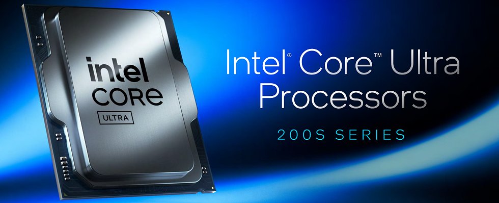
The time has finally come and the results for Intel’s new Core Ultra 200 series are on the table. I can already spoil the fact that we will see very interesting, but partly mixed results today compared to AMD’s Ryzen 9000 series, especially in the gaming sector. The tension curve was also extremely tense for me and so it ended up as it had to under such circumstances: perplexity, astonishment, joy and disappointment as a quartetto infernale in good company. And so pretty much all the testers were in the dark for a long time…
The right media kit from MSI
MSI also provided us with an exclusive media kit for this test, which included a Core Ultra 9 285K, an MSI MEG Z890 Ace, DDR5 8400 Kingston Fury and, of course, the matching AiO compact water cooling system in the form of the Core Liquid. I then used the mainboard, the RAM, the CPU and of course the AiO for the tests straight away, as it was like food on wheels because everything fitted together so perfectly. I will probably always remember the CPU gripper as a nice gimmick. You have to come up with it first. I didn’t miss it until I used it for the first time. Now I do.


The CPU in detail
But back to the topic of Intel. The new CPUs are certainly impressive in synthetic benchmarks, but gaming in particular unfortunately showed a completely different dynamic. AMD’s Ryzen 9000 series, especially models such as the 9950X, are particularly strong in many games thanks to their improved architecture and high single-core performance, especially on the new X870E mainboards, with the new UEFI and all driver updates under Windows 11 24/H2. But today it’s all about Intel…

While Intel’s hybrid architecture with P and E cores offers advantages in multithreading, gaming often tends to benefit from strong single-core performance and high cache performance. Here, AMD with its higher L3 cache capacity (64 MB versus Intel’s 36 MB) certainly remains more than evenly competitive, which can lead to advantages in games that depend on cache-intensive processes. The best example is the Ryzen 7 7800X3D, which will play a special role in this respect. But more on this in the test. And if anyone wants to count the 1851 pins, have fun:
|
|
 |

Technical features of the Arrow Lake architecture
Below you will find a link to a previously published article that contains all the details that Intel shared with us in advance. I don’t want to repeat this redundantly here. Instead, I would like to briefly supplement this content before moving on to the tests. The main components of the CPU, we remember, consist of six tiles that fulfill different tasks. These tiles are manufactured using different semiconductor processes from different manufacturers. One of the most important innovations is the compute tile, which integrates both the P-cores (performance cores) and the E-cores (efficiency cores). These cores are based on the new Lion Cove (for the P-cores) and Skymont (for the E-cores) architectures. We also know that the compute tile is manufactured in the TSMC N3B process, which is new for Intel CPUs, as previous processors were based on Intel’s own 10nm technologies. In total, the compute tile contains up to 8 P-cores and 16 E-cores, which results in a higher power density than previous generations. The integration of the cores on a common tile also improves the connection through a ring bus, which enables more efficient communication between the cores.
In addition to the compute tile, there is also a graphics tile that is manufactured using the TSMC N5P process. This tile contains four Xe LPG graphics cores of the “Alchemist” architecture. There is also an SoC tile that integrates various systems on one chip, such as the DDR5 memory controller and the PCIe 5.0 controller for connecting a discrete GPU. Compared to the previous Intel generations, such as Alder Lake and Raptor Lake, Arrow Lake thus shows some significant differences. While Alder Lake and Raptor Lake also relied on a hybrid architecture with P and E cores, these cores were housed in two separate areas of the compute tile. With Arrow Lake, however, the P and E cores are combined, which improves connectivity and thermal management. I have now tabulated and exemplified the whole thing for the Core Ultra 9 285K:
| Tile | Process | Function | Additional details |
|---|---|---|---|
| Compute tile | TSMC N3B | Contains the P and E cores (Lion Cove and Skymont) | 8 P-cores, 16 E-cores, ring bus interconnect |
| Graphics tile | TSMC N5P | Contains the Xe-LPG “Alchemist” graphics cores | 4 graphics cores |
| SoC tile | TSMC N6 | Controls memory and I/O | DDR5 memory controller, PCIe 5.0 x16, NPU, video engine (H.264/H.265/AV1) |
| I/O tile | TSMC N6 | Connects memory and external devices | PCIe 5.0 x4 (SSD), PCIe 4.0 x4 (SSD) |
| 2x filler tiles | Not specified | Structural stability for the heatspreader | Provides a gap-free surface for the heatspreader |
| Base tile | Intel 1227.1 | Connects the various tiles | Central node for connecting the tiles |
While the compute tile is based on the latest TSMC N3B process, older and less cost-intensive manufacturing technologies are used for other tiles. This should enable Intel to reduce manufacturing costs, as the particularly expensive new manufacturing processes are only used where they are really needed.
Thermal features
Another new feature is the use of two filler tiles. A filler tile is a tile that has no active function but serves as a placeholder. These filler tiles are used to mechanically or thermally balance the chip, especially in designs that are customized for different markets or use cases. The aim is to optimize the integration of the individual functional tiles on the chip and to ensure even heat distribution or mechanical stability. They thus also ensure that the heatspreader, which dissipates the heat from the CPU, rests on a flat surface. This is to prevent the heatspreader from bending or being damaged, which could lead to the CPU overheating. Speaking of heatspreaders, the cooler industry should also be guided by the decentralized hotspots, which also differ slightly between the various models:
| 8P 16E | 6P 8E |
 |
 |
I did the complete Arrow Lake S tests with a matching MSI MAG CoreLiquid AiO compact water cooling system, which takes exactly these hotspots into account with a special bracket. I can fully confirm MSI’s measurements (see picture below), as I also experimented with the new and the old Uni-Bracket and measured significant differences that go beyond the usual tolerance limits:

MSI has found a kind of compromise for the complete series and places the pump housing at the intersection of both hotspots to cover as much as possible, but with the focus on the larger and therefore also hotter models. I have illustrated what this looks like in a separate superposition:

And for the very inquisitive and / or forgetful, there’s also the foiled deep dive through the Intel architecture. That should be enough of an introduction for now.
Intel Arrow Lake S and H in brief: Significantly higher efficiency, cooler and not slower

- 1 - Introduction and imprtant details
- 2 - Test setup and methods
- 3 - Gaming Performance HD Ready (1280 x 720 Pixels)
- 4 - Gaming Performance Full HD (1920 x 1080 Pixels)
- 5 - Gaming Performance WQHD (2560 x 1440 Pixels)
- 6 - Autodesk AutoCAD 2023
- 7 - Autodesk Inventor 2021 Pro
- 8 - Rendering, Simulation, Financial, Programming
- 9 - Science and mathematics
- 10 - Workstation: power consumption and efficiency
- 11 - Gaming: power consumption and efficiency
- 12 - Summary and conclusion


202 Antworten
Kommentar
Lade neue Kommentare
Veteran
Veteran
Urgestein
Veteran
1
Veteran
Urgestein
Neuling
Urgestein
Mitglied
Veteran
1
1
Veteran
Urgestein
1
Urgestein
Urgestein
Mitglied
Alle Kommentare lesen unter igor´sLAB Community →