


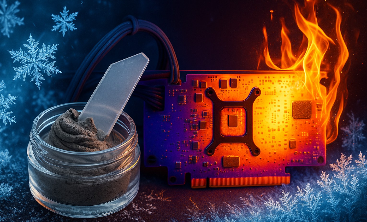
In this article, I deliberately do not want to follow the common expectation of judging the performance of a thermal interface material based on individual Kelvin or supposed peak values. Such comparative figures often appear more precise than they actually are in a real system. The decisive factor is not the isolated thermal conductivity of a pad or putty, but its actual influence on the interaction between component, PCB and the surrounding cooling paths. A TIM only ever works within the limits set by the package, the PCB and the geometrically available surfaces, and this is precisely where the decisive factors for the thermal load of modern electronics lie.
The structure of current DrMOS and SmartPowerStages shows very clearly that the majority of waste heat is dissipated via the PCB and not via the top of the housing. A TIM does not improve this path, but primarily creates a defined mechanical coupling and stabilizes local hotspots, which together determine the ageing of materials. Its role is often overestimated because the thermal bottlenecks do not lie in the TIM, but in the internal housing structure of a DrMOS and in the limited thermal conductivity of the PCB itself. However, the available surface area is even more underestimated, as it determines how well the PCB can distribute heat and transfer it to other coolers or a backplate.
The backplate in particular is often only perceived as a mechanical component, although it has a central thermal function. Its large-area connection via a pad makes it possible to actively include the rear of the PCB in the cooling network. It lowers the temperature of the entire VRM zone, stabilizes adjacent components and influences the long-term ageing behaviour of solder joints and plastic housings. The effect of a pad therefore arises less from its high nominal thermal conductivity than from the area that it makes thermally usable and from its ability to dissipate heat across both sides of the PCB.
These relationships not only apply to MOSFETs, but can also be transferred to GDDR6(X) and GDDR7 modules in a broader sense. There, too, the path via the PCB is dominant, and there, too, the importance of the thermal conductivity of a pad is overestimated, while the role of the surface area and the cooling on both sides is often underestimated. The overall system is always decisive, not the individual value. I would therefore like to deliberately shift the focus of this article away from individual key figures and towards a systemic view. Today I will show how heat is distributed in a real VRM and memory environment, which paths actually dominate and why surface area, PCB and backplate are more important for the thermal stability and ageing of a system than the pure thermal conductivity of a TIM.
It is a continuation of an article I had already written on this topic. Some of the pictures will therefore be familiar to you. But the approach today is completely different and much more in-depth. Because if the heatsink is no good, you can’t save anything by using gold as a TIM. And an oversaturated PCB becomes a bottleneck all the more.
For precisely these reasons, I expressly do not want to use the extreme case of the PNY RTX 5070 measured at the time, the back of which reached up to 107 °C locally. This outlier was caused by an unusual oversaturation of the PCB and the overlapping of several hotspots, which even reversed the heat flow in some places. Such conditions are rare in practice and tend to distort the view of the fundamental relationships. To understand the cooling of modern voltage converters, it is more useful to focus on typical cases in which the waste heat follows clear and reproducible paths. This is exactly what I want to focus on today, and I would also like to show that there are often more important adjustment screws than particularly expensive pads or exotic puttys.
Problem: Hotspots in the voltage converters and the current path to the GPU
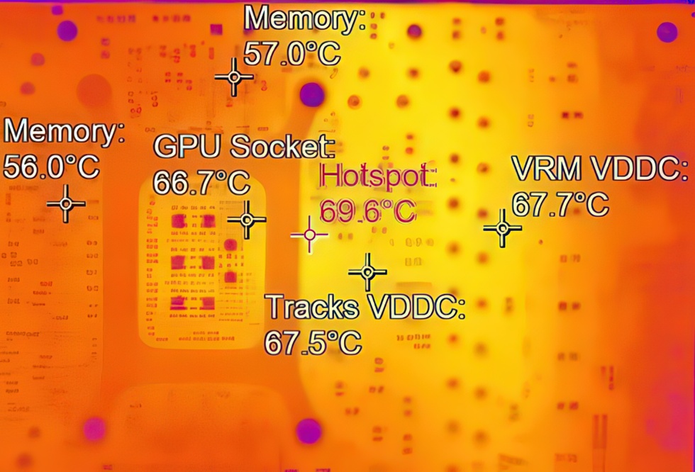
I will now go through the analysis with you step by step using an MSI GeForce RTX 5070 Ti Ventus, so that the rear side becomes thermally tangible and can be clearly linked to the front side (mirrored upside down). This also makes it easy to understand why hotspots occur exactly there, where around 67 to 70 °C are visible in the IR image, although the GPU itself is operated moderately in this scenario. The IR image of the back of the board shows a clearly structured thermal distribution. Without extreme stress and without the notorious overlapping of several hotspots, as occurred in the 107 °C case of the other card, the temperature image is structurally well usable. Several zones stand out.
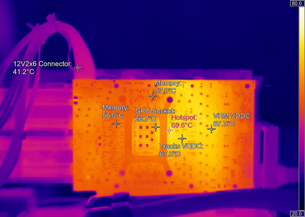
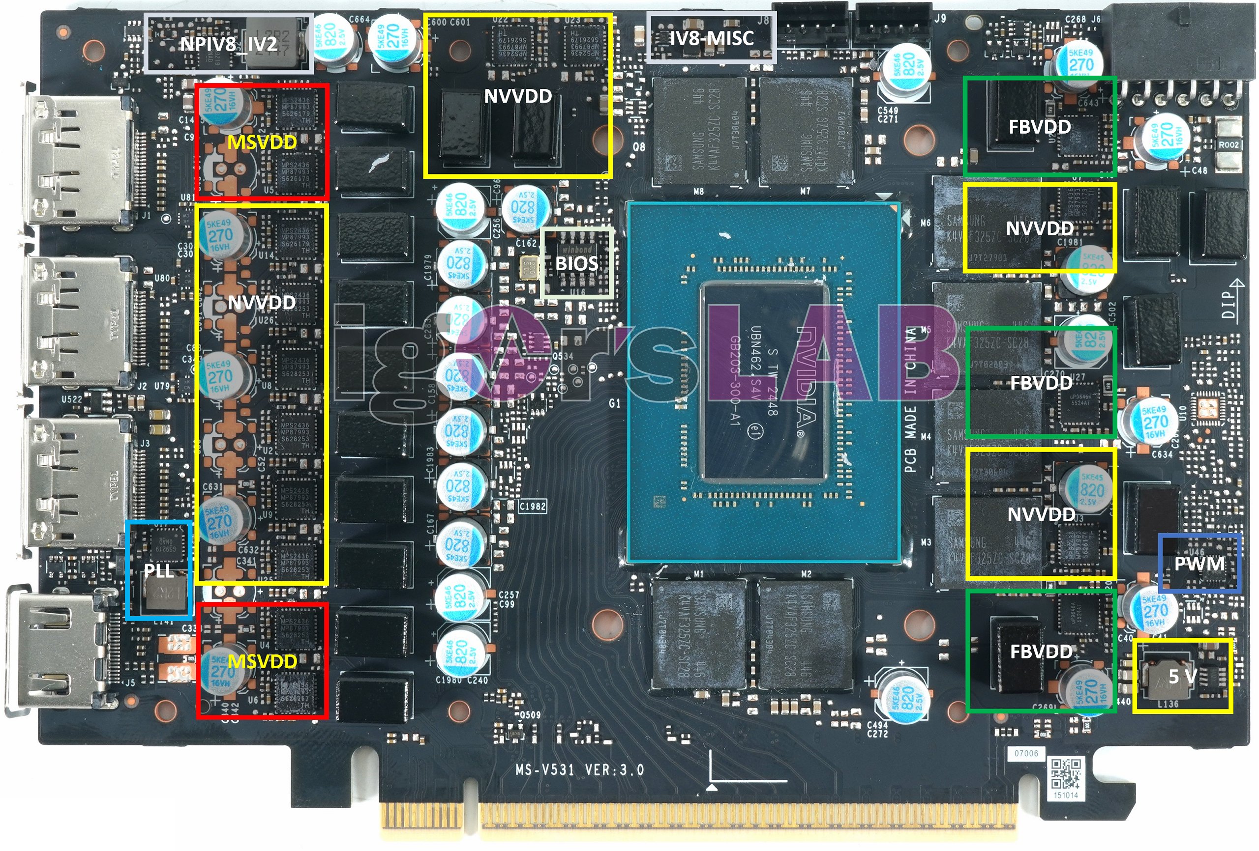
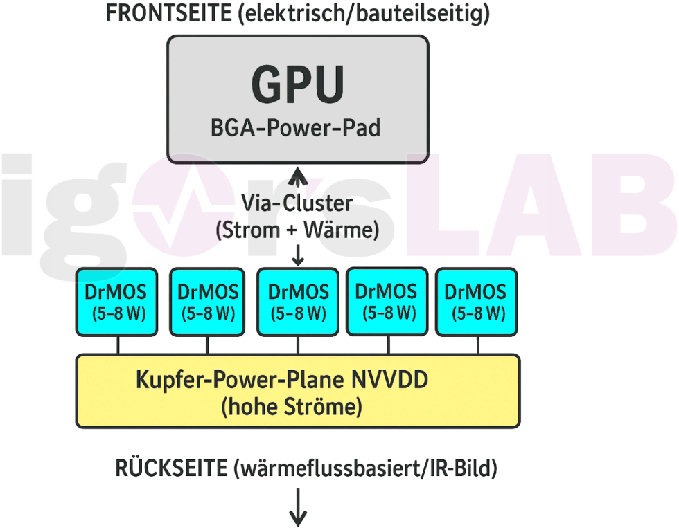
The warmest areas are around 69.6 °C at the hotspot, 67.7 °C VRM VDDC, 67.5 °C for the tracks VDDC, 66.7 °C at the GPU socket and 57 °C for memory. It is striking that the hotspot is almost exactly in the keel line of the VDDC supply of the GPU. This is the classic VCore rail NVVDD (marked yellow on the front). These rails carry by far the highest currents on the board, and the PCB is stressed in this area both by the ground path of the DrMOS devices and by the massive current flow in the copper rails and vias.
The “VRM VDDC” and “Tracks VDDC” areas in particular form a coherent thermal fingerprint: the IR hotspot superimposes the energy dissipation through the PCB on the current path from the DrMOS to the GPU. The approximately 67 to 70 °C are still normal in themselves, but they show exactly where the power dissipation from several sources converges. If you mentally mirror the IR image horizontally and superimpose it on the front, the central hotspot ends up directly behind the NVVDD phases of the GPU, which are arranged in pairs. The yellow markings on the front show it very clearly: three NVVDD groups of two flank the GPU socket. The 69-degree hotspot is located exactly behind this zone in the IR image.
The cause is twofold:
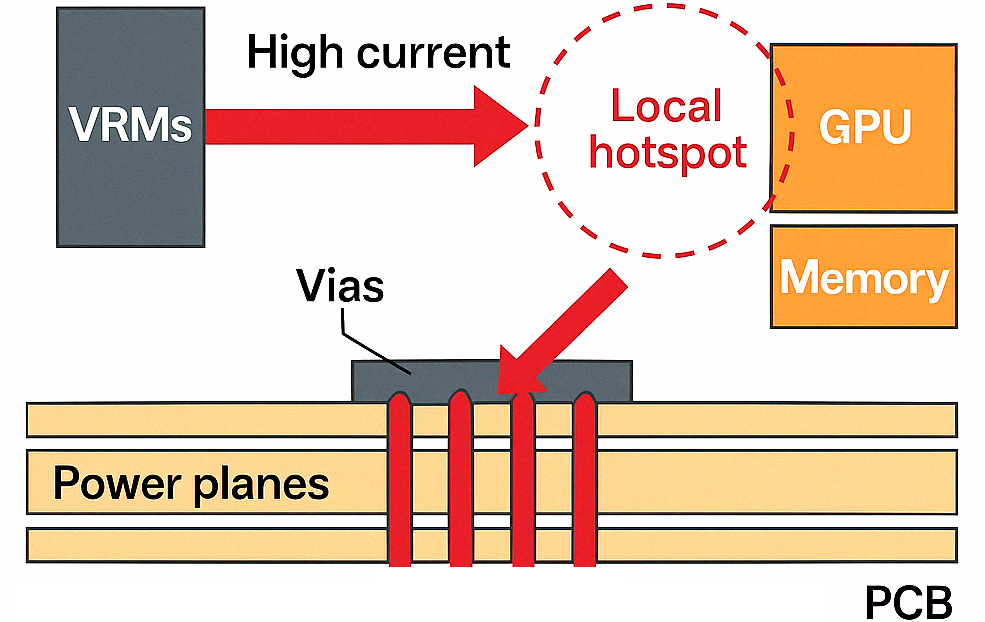
First, the majority of the power dissipation of a DrMOS (60 to 80 percent) goes into the PCB via the ground path. The FR-4 absorbs this heat poorly and hardly dissipates it to the side. It therefore accumulates in the immediate vicinity of the component.
Secondly, after the DrMOS, the entire GPU supply current runs via several parallel copper traces and a large number of vias into the internal GPU BGA structure. Each of these metallic elements contributes current-related ohmic losses. They also heat the PCB directly and locally at the bottlenecks.
This creates a thermal double peak: under each VDDC DrMOS and on the subsequent copper rails up to the GPU. Accordingly, “VRM VDDC” and “Tracks VDDC” show almost identical temperatures.
Analyzing the cause along the current path
If you look at the widened copper surfaces of the NVVDD rail, the correlation becomes clearer. The VDDC phases are connected to the GPU pad several times via large copper layers and powerful via arrays. The currents are considerable; depending on the second, several hundred amperes can run through the rail. The ohmic loss in conductor paths, vias and transitions is small per unit, but noticeable in total. This results in the typical sequence of heat loss sources:
– MOSFET switching losses
– MOSFET conduction losses
– Coil losses (low in this case)
– Conductor losses (copper fill areas)
– Via clusters (local bottlenecks)
– GPU-BGA power region
If you compare the IR image with the front of the PCB, the greatest heat is concentrated at precisely these points. Not through a single component, but through the sum of many small effects.
Why does the VRM area stand out so much?
The MSVDD and FBVDD areas are also warm, but well below the main rail. These rails carry much less current, so there are fewer ohmic board losses. The VRM temperature of the NVVDD rail, on the other hand, is a reflection of two things: the typical power dissipation of the many DrMOS and the current density of this rail. The vias under the NVVDD phases are central here. If they are projected onto the rear side upside down, the hotspot falls almost congruently over the via pad clusters. It is precisely these that conduct the heat downwards and define the bottom path of the thermal resistance.
The images of the front show that the NVVDD rail is routed over a fairly narrow width, but that the copper surface is not distributed over a sufficiently large area at the bottom. Although the vias are present in groups, they are not optimized for large-area heat distribution, but are mainly arranged for electrical current transmission. Such electrical vias are placed for electrical impedance, not for good heat distribution. There are conductive surfaces between these elements, which have a clean electrical structure but only limited thermal cross-sections. As a result, not only high currents flow in these areas, but also undesirable parasitic currents, some of which generate additional losses at the via junctions. These transition losses are small, but can add up with nine phases, especially if thermally relevant vias are not widely distributed but concentrated in groups. The IR image indicates precisely this superposition, as the hotspots are not point-shaped, but rather band-shaped.
A third point results from the other supply rails. The MSVDD rails also generate their own losses, which spread through the PCB in the direction of the NVVDD zone. This leads to an effect that acts thermally like a superposition. The VRM waste heat from the GPU is not dissipated in isolation, but is underpinned by lateral heat flows from the auxiliary rails. The layout itself clearly shows this neighborhood, and the IR image confirms this thermal mixing. The central hotspot on the rear side is therefore not only caused by the many NVVDD phases, but also by the power losses from coils and small driver components of adjacent rails feeding in from the side.
In addition, the NVVDD phase is located at a point on the PCB where several current paths converge. High currents always mean heating in the copper tracks, especially at their bottlenecks such as layer changes, vias and copper tapers. Such bottlenecks are often electrically unavoidable, but thermally critical. The IR image shows that the rear side makes these bottlenecks visible, because the hottest areas coincide very precisely with geometric constrictions and layer transitions of the core rail, which are marked on the front side.
This creates the typical image of a superimposed heat source. The VRM waste heat is the actual main source, but the heating is flanked by additional ohmic losses distributed in the metal layers, by via bundles and by neighboring rails. The combination of high power density, segmented thermal vias and a current-guided layout creates a highly thermally focused pattern on the backside. Many of these structures are of course subject to technical constraints.
What I can say for sure, however, is that the thermal performance of this area of the board is more limited by the geometry than it needs to be, and that VRM heating is not visible in isolation as a result, but is superimposed on parasitic loss paths of the PCB. This results in an overall higher temperature level in the VRM zone, which is clearly reflected in the IR image. And that’s what we want to calculate today.
Why exactly this temperature image is created
If you superimpose the two images in your mind’s eye and trace the course of the power supply, the following chain emerges:
– DrMOS generates around 5 to 8 watts per phase
– 60 to 80 percent of this power goes into the circuit board
– Copper surfaces under the DrMOS heat up immediately
– Vias transport current, but only a minimal amount of heat
– The GPU current path generates additional ohmic heat loss
– This is added directly above the GPU power region
– The result is a wide hotspot area in the IR imageThe hotspot at 69.6 °C in the IR image is therefore the tip of a purely board-based temperature massif, which is made up of switching losses and ohmic track losses.
The hotspot formation is primarily a current path image, not a pad or putty problem!
In this case, the backside “burns” exactly where the GPU current flows. The VRM itself supplies most of the thermal energy, the traces and via nets distribute it and generate additional resistive losses. This is a structural issue of layout and component distribution, not just a thermal pad or backplate issue. I apologize in advance for the following theory, but I sat down on the stairs of a construction trailer in dungarees to keep it from being too complex. So don’t worry, you don’t even need high school diploma knowledge here. 🙂


11 Antworten
Kommentar
Lade neue Kommentare
Mitglied
Urgestein
Urgestein
Mitglied
1
Urgestein
1
Urgestein
Urgestein
Veteran
Urgestein
Alle Kommentare lesen unter igor´sLAB Community →